


I. Introduction
As the saying goes, if the foundation is not solid, the mountains can be shaken. If you want to learn MCU well, you must be very familiar with the basic principles. After all, we are developing at the bottom level, so the lower the level, the better. It will let us know what each line of code is doing. The essence is actually to operate the registers, let the single chip microcomputer complete the action we want, such as lighting an LED light, and the library function development of stm32 is no exception. It just encapsulates the operation registers into functions. We only need to configure the parameters of the specified function. , and then call this function to automatically configure the corresponding registers. In fact, the essence is to operate the registers, which is more convenient and quicker. If you only learn library functions, you will feel like a loft in the air later, knowing what it is and not knowing why.
Summary: Registers must be learned. If it is a bit difficult to learn in the early stage, you can learn library functions for a while and look at the registers after returning, which will be much better;
Two. STM32 system architecture
The STM32 chip is a packaged finished product, mainly composed of the core and on-chip peripherals. If compared with a computer, the core and peripherals are like the relationship between the CPU and the motherboard, memory, graphics card, and hard disk on the computer.
The following diagram of the stm32 system structure is very important. We need to understand how stm32 works and which bus each peripheral is mounted on. What we mainly study is the peripherals mounted on the AHB system bus.
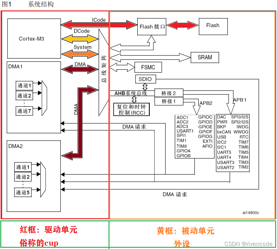
1. Four drive units (CUP)
Cortex™-M3 core DCode bus
Cortex™-M3 core system bus System
GMDMA1
GMDMA2
2. Four passive units (peripherals)
Internal SRAM
Internal flash memory FLASH
FSMC
AHB to APB bridge, which connects all APB peripherals
3. Drive unit
ICode bus
The I in ICode means Instruction, which is the instruction. The core reads the internal FLASH code instructions through the ICode bus to execute the program.
DCode bus
D in DCode means Data, that is, data, which means that this bus is used to fetch numbers. Because data can be accessed by Dcode bus and DMA bus (fetching data from flash, SRAM, or peripheral data registers), in order to avoid access conflicts, a bus matrix is required to arbitrate when fetching data to determine which bus is fetching The fetched data can be temporarily stored in the registers in the Cortex™-M3 core for processing.
System bus System
The system bus mainly accesses the registers of peripherals. We usually refer to register programming, that is, reading and writing registers are all done through this system bus.
DMA bus
The DMA bus is mainly used to transmit data like the DCode bus, but the Dcode bus transfers data to occupy core (cpu) resources, and the DMA bus is equivalent to being independent of the core cpu but helping the core cpu to transfer data without occupying the core (cpu) Resources, that is, the core cpu can do other things such as light up an LED light while DMA is transferring data
bus matrix
The bus matrix coordinates the access arbitration between the kernel system bus and the DMA master bus, and the arbitration uses a round-robin algorithm. Because the data can be accessed by the Dcode bus and the DMA bus, the data can be in the data register of a certain peripheral, in the SRAM, or in the internal FLASH. Therefore, in order to avoid access conflicts, a bus matrix is required to arbitrate when fetching data to determine which bus is fetching data.
4. Passive unit
Internal FLASH
Briefly introduce the content stored in the flash: After the compiled program we write is compiled one by one instruction (binary code), it is stored in FLASH, and the const keyword modification in our constant or constant variable C language is also stored in FLASH
Internal SRAM
It is the computer memory stick we often say, the local variables and global variables inside the program function, the overhead of the heap (malloc allocation) stack (local variables), etc. are all based on the internal SRAM. The core accesses it through the DCode bus
FSMC
The full English name of FSMC is Flexible static memory controller, which is called a flexible static memory controller. It is a very distinctive peripheral in STM32F10xx. Through FSMC, we can expand memory, such as external SRAM, NANDFLASH and NORFLASH. But one thing we should pay attention to is that FSMC can only expand static memory, that is, S: static in the name, and cannot be dynamic memory, such as SDRAM cannot be expanded.
AHB to APB bridge
Two AHB/APB bridges provide simultaneous connection between AHB and 2 APB buses. The operating speed of APB1 is limited to 36MHz, and APB2 operates at full speed (up to 72MHz), and various featured peripherals of STM32 are mounted on it. The GPIO, serial port, I2C, and SPI peripherals we often say are mounted on these two buses. This is the focus of our learning STM32, which is to learn to program these peripherals to drive various external devices.
3. Memory Mapping
The memory itself does not have address information. Its address is assigned by the chip manufacturer or user. The process of assigning an address to the memory is called memory mapping. If another address is assigned to the memory, it is called memory remapping.
Program memory, data memory, registers, and I/O ports are organized in the same 4GB linear address space. Data bytes are stored in memory in little-endian format. The lowest address byte in a word is considered the least significant byte of the word, and the highest address byte is the most significant byte.
1. Storage space of STM32
The 4GB mentioned above, but why is it 4GB, the size of the storage space is determined by the number of address buses in the CPU on the chip, and the number of buses inside the stm32 chip is 32
The memory is divided into memory units one by one. The size of each memory unit is one byte. In order to effectively access each unit of the memory, the memory unit is numbered. The number is called the address of the memory unit.
how to generate address
32 address lines each can output positive and negative (1 or 0)
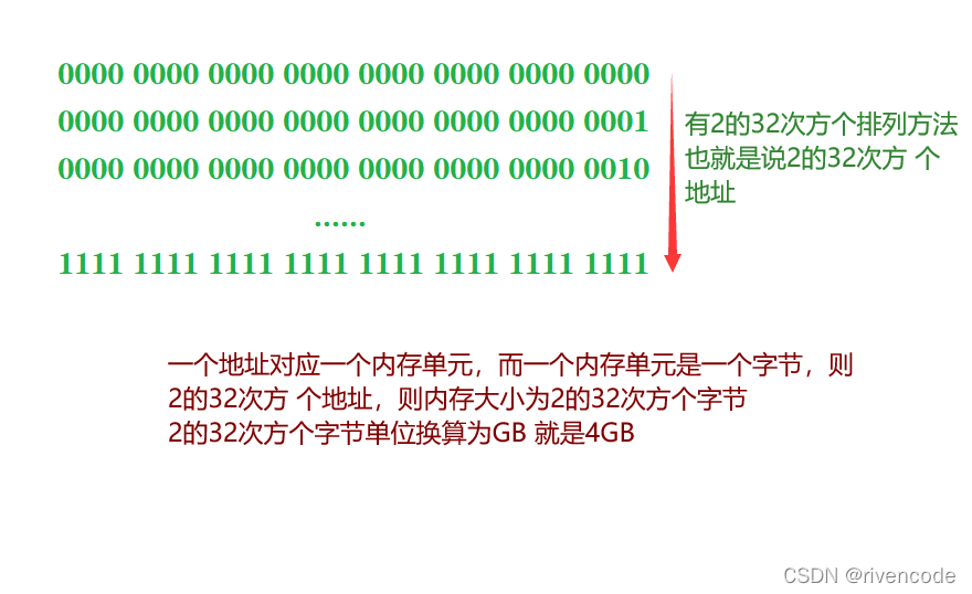
After the address is allocated, the FLASH, RAM, FSMC and bridge from AHB to APB of the controlled unit (that is, on-chip peripherals), these functional components are arranged together in a 4GB address space. When we are programming, we can find them by their addresses, and then operate them (the address dereferencing operation in C language * take out the content to read and write data to them).
2. Functional division of the memory area
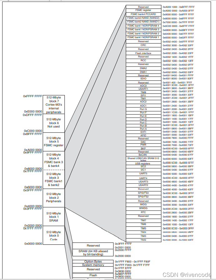
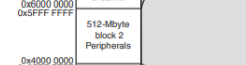
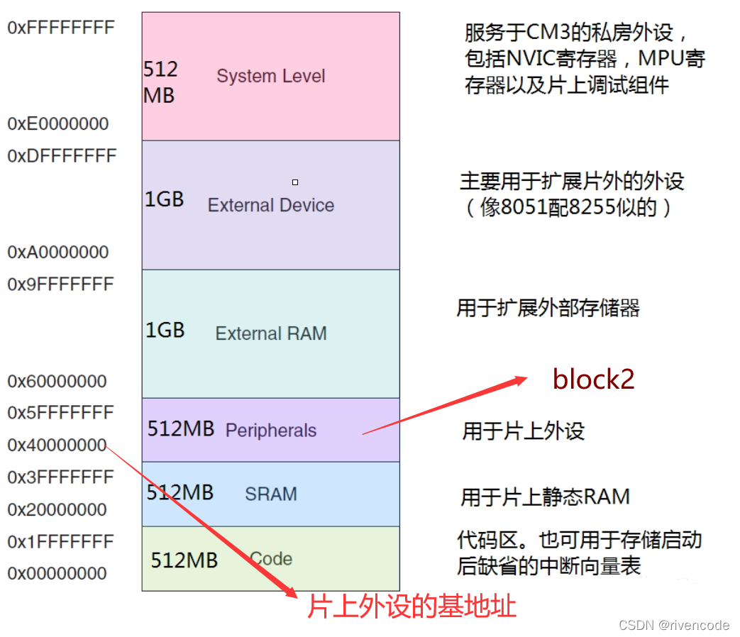
In this 4GB address space, ARM has been roughly divided into 8 blocks on average, each block is 512MB, and each block also has a specified purpose. The size of each block is 512MB, which is obviously very large.
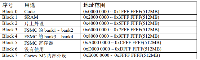
Among these 8 Blocks, 3 blocks are very important, and they are also the three blocks we care most about. Block0 is used to design internal FLASH, Block1 is used to design internal RAM, and Block2 is used to design on-chip peripherals. Below we briefly introduce the functional division of specific areas in these three Blocks.
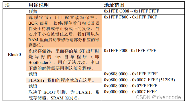
Functional division of memory Block0 internal area.
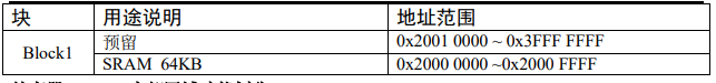
Functional division of internal area of memory Block1
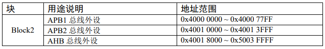
Functional division of the internal area of memory Block2
Block2 is used to design the on-chip peripherals. According to the different bus speeds of the peripherals, the Block is divided into two parts: APB and AHB. APB is further divided into APB1 and APB2.
Explain the reserved addresses, these addresses do not allocate storage units to him, the theory is 4GB but in reality there are not so many, it just gives you indicators and does not use them all
3. What is a register
1. Register map
In the area of memory Block2, on-chip peripherals are designed. They use four bytes as a unit, a total of 32 bits, and each unit corresponds to a different function. When we control these units, we can drive the peripherals to work. We can find the starting address of each unit, and then use the C language pointer operation method (since a unit is four bytes, we use a four-byte pointer (int *) to operate these functional units) To access these units, if it is accessed through this address every time, it is not only bad to remember but also prone to errors. At this time, we can give this memory unit an alias in the name of function according to the function of each unit. , the process of aliasing a memory unit with a specific function that has been assigned an address is called register mapping.
2. What is a register
Register: an alias for a unit with a specific function. This alias is called a register, so a register is just the name of a unit with a specific function.
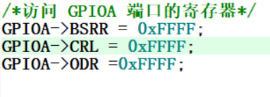
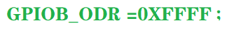
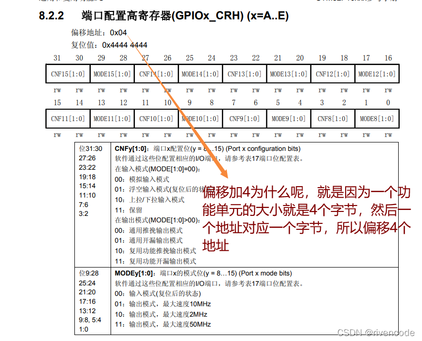
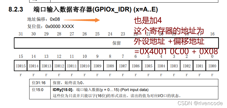
For example, we find that the address of the output data register ODR of the GPIOB port is 0x4001 0C0C (as for how to find this address, you can skip it first, we will explain in detail later), the ODR register (that is, the 4-byte functional unit) is 32bit, The lower 16 bits are valid, corresponding to 16 external IOs, and the IO corresponding to writing 0/1 will output low/high level. Now we use the C language pointer operation method to make all 16 IOs of GPIOB output high level, see for details.
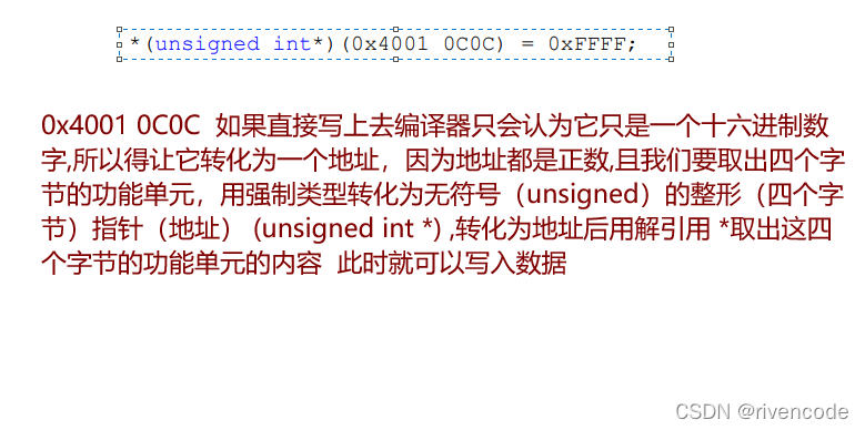
3. How to alias the functional unit (register)
We use #define in C language to define a register identifier
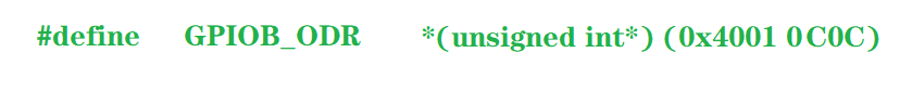
In this way, it is much simpler to operate one more functional unit, and it is easier to understand
The next step is to find all the functional unit addresses of the GPIOB port layer by layer, change their aliases into registers according to different functions, and directly operate the corresponding registers in the future.
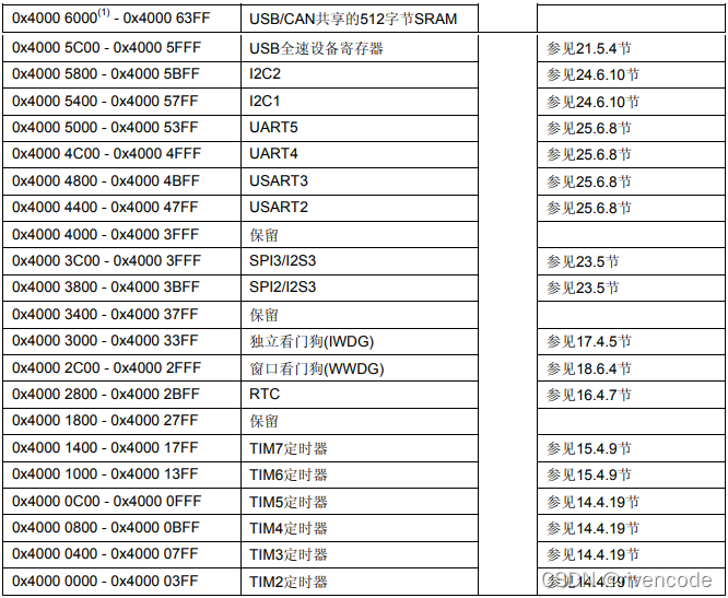
4. Peripheral address mapping of STM32
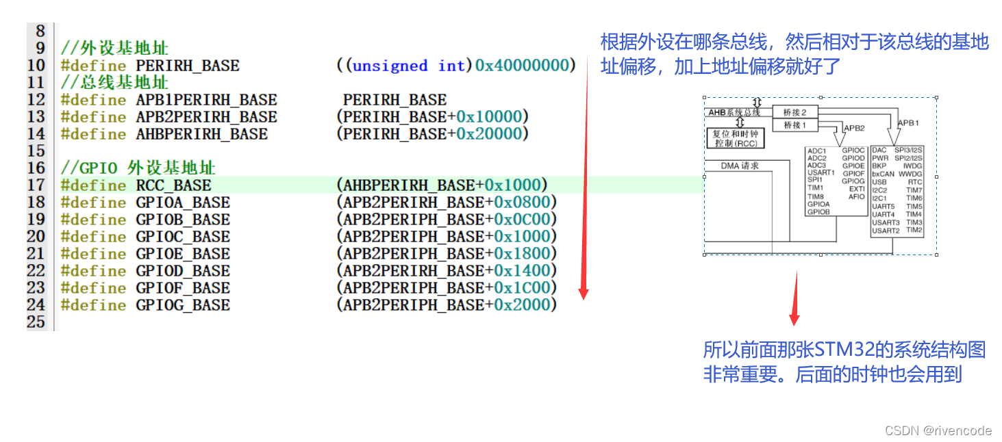
The on-chip peripherals are divided into three buses. According to the speed of the peripherals, different peripherals are mounted on different buses. APB1 mounts low-speed peripherals, and APB2 and AHB mount high-speed peripherals. The lowest address of the corresponding bus is called the base address of the bus, and the base address of the bus is also the address of the first peripheral device mounted on the bus. Among them, the address of the APB1 bus is the lowest, and the on-chip peripherals start here, also called the peripheral base address.
Lists the start addresses of the built-in peripherals in the STM32F10xxx used.

Here I intercept a section to teach you how to find the bus base address and peripheral base address.
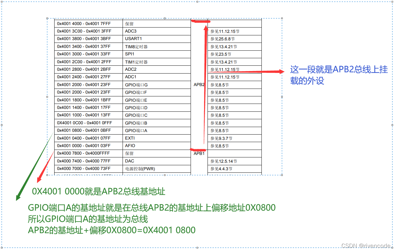
Look at the picture above and you can find the base addresses of the following buses or peripherals one by one.
bus base address
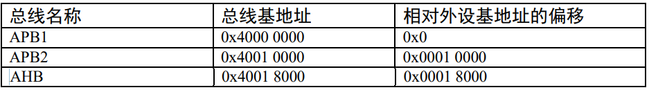
Relative peripheral base address offset” is the difference between the bus address and the “on-chip peripheral” base address 0x4000 0000.
Peripheral base address
Various peripherals are mounted on the bus, and these peripherals also have their own address ranges. The first address of a specific peripheral is called “XX peripheral base address”.
Here, GPIO is taken as an example, other peripherals are the same operation
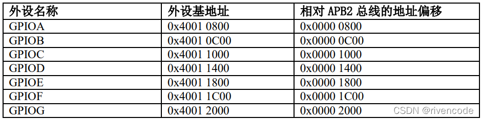
Here, relative to the address offset of the APB2 bus, the peripheral base address minus the APB2 bus base address 0X4001 0000 is the address offset relative to the APB2 bus, because all GPIO ports are mounted on the APB2 bus.
Peripheral Registers
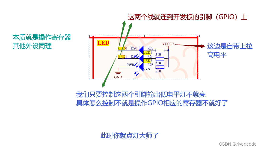
In the address range of the XX peripheral, the registers of the peripheral are distributed. Taking the GPIO peripheral as an example, – GPIO (general purpose input output) is the abbreviation of the general purpose input and output port. Simply put, it is a pin that can be controlled by STM32. The simplest application is to connect the GPIO pin to the cathode of the LED light, connect the anode of the LED light to the power supply, and then control the level of the pin through STM32, so as to control the LED light on and off.
Here we take the GPIOB port as an example to illustrate what registers GPIO has.
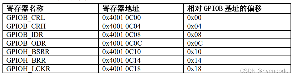
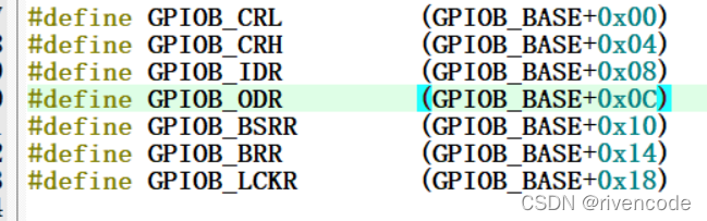
GPIO has many registers, each with a specific function. Each register is 32bit, occupying four bytes, arranged in order on the base address of the peripheral, and the position of the register is described by the offset address relative to the base address of the peripheral.
The address of each register = the base address of the peripheral + the offset of the register relative to the base address of the peripheral
Here we look at several registers in order of address offset, and understand the description of the registers, as shown in the figure
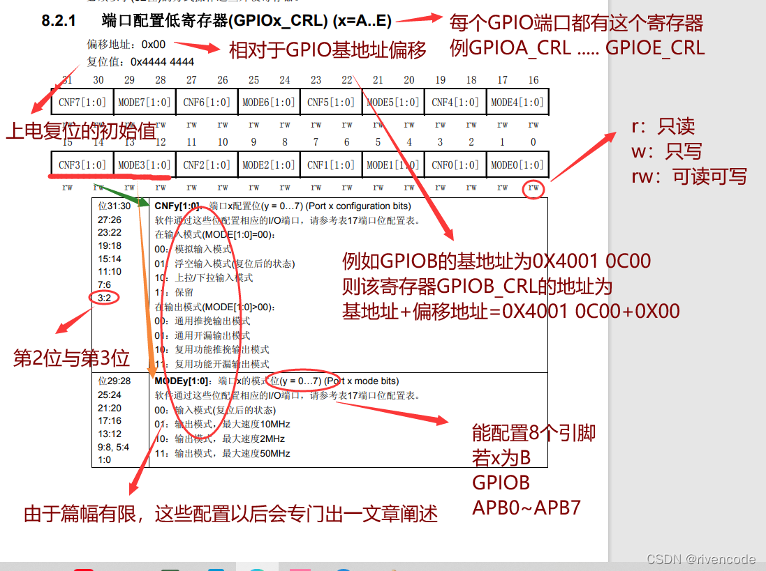
I won’t list them one by one here. All peripherals basically have their own registers, but they are arranged according to this pattern with different functions and names.
Four. C language encapsulation of registers
The above method is not convenient enough. Next, through layers of dolls, find the address of each peripheral register and then encapsulate it with a C language structure
1. Package bus and peripheral base address
In order to facilitate understanding and memory in programming, we define the bus base address and peripheral base address with corresponding macros, and the bus or peripherals use their names as macro names.
2. Package register list
The address of each register = the base address of the peripheral + the offset of the register relative to the base address of the peripheral
So far, have you found that the address of a characteristic register is offset by 4 each time, if the type of a register is defined as (unsigned int), does it occupy exactly 4 bytes in memory, and a memory unit is 1 byte, Allocate an address, the 4 bytes are not exactly offset by 4 addresses each time, and there is memory alignment that conforms to the structure. I will not go into details about the memory alignment of the structure here, and I will elaborate on the article about the structure in the future.
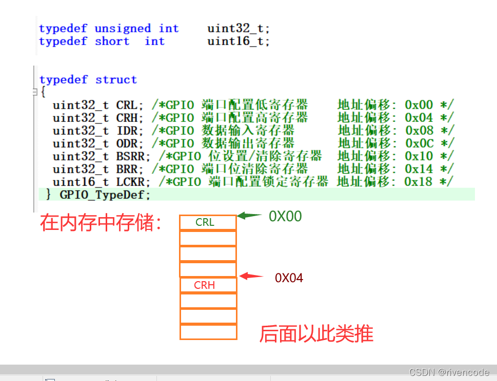
After encapsulating the registers into a structure, the next step is to take out the registers to operate on the registers. Taking GPIOA as an example, we will force the base address of the GPIOA peripheral into the first address of the structure. Isn’t it a perfect solution?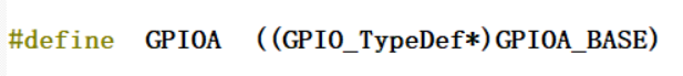
For the GPIO_TypeDef we defined, the first address of this structure is 0x4001 0800 (this is also the address of the first member variable CRL), then the address of the second member variable CRH in the structure is 0x4001 0800 +0x04, plus The 0x04 in this is the offset of the 4 byte address occupied by the CRL, and the offset of other member variables relative to the first address of the structure
3. Operation register
Finally, we can directly use the macro to define the GPIO_TypeDef type pointer, and the pointer points to the first address of each GPIO port. When using it, we directly use the GPIOA pointer to access the structure member register